
Hardware Reverse Engineering#
Hardware reverse engineering reconstructs how a device is built: its power domains, processors, memories, communication paths, and test interfaces. The result is an annotated board map that explains where firmware is stored, how external inputs reach the processor, and which interfaces can support further analysis.
Inspect the Board and Connectors#
Photograph both sides of the printed circuit board (PCB), record board and component markings, and distinguish populated components from unpopulated footprints. Missing components may reflect a product variant, manufacturing option, or test provision; an empty header alone does not identify a debug interface.
Trace connector pins through protection components, filters, and transceivers to the processor. Connector size and position are clues; establish the pinout from continuity measurements and component documentation.
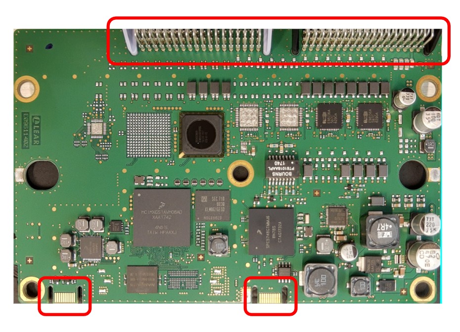
Fig. 1 Connector and component placement provides the starting point for a board map.#
Power Domains and Startup Conditions#
Inductors, capacitors, regulators, and protection devices help locate the power-supply path. A board may use switching regulators, linear regulators, or both, with separate rails for the processor core, I/O, transceivers, and standby logic.
Identify ground, supply inputs, expected voltages, enable signals, and reset/watchdog dependencies before powering an unfamiliar board. Use the confirmed pinout and a current-limited bench supply. A device that repeatedly resets may be missing a wake-up condition or watchdog response rather than having corrupt firmware.
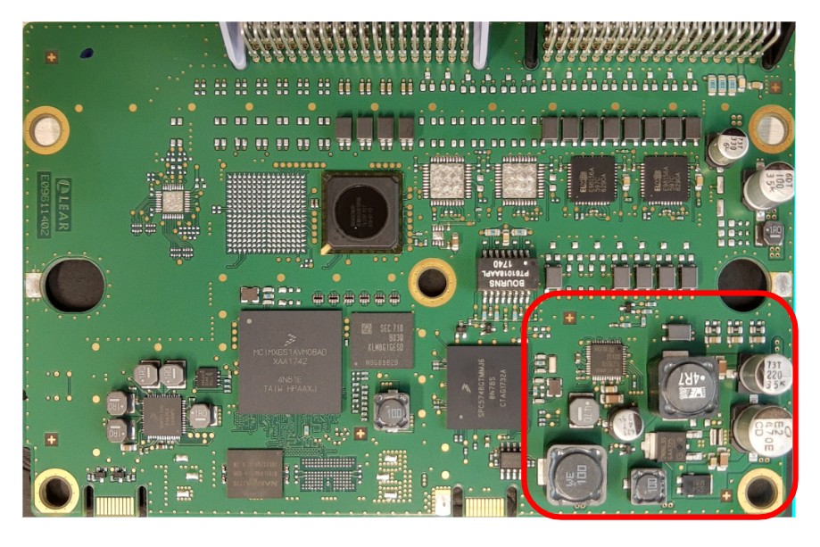
Fig. 2 Identify the input protection and regulator stages before tracing the individual supply rails.#
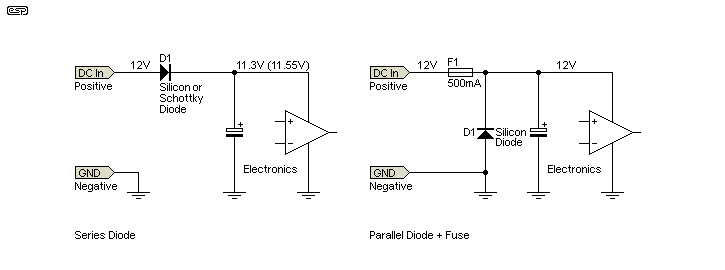
Fig. 3 Examples of reverse-polarity protection. Source: Elliott Sound Products, Application Note 013.#
Filters, Chokes, and Transformers#
A common-mode choke contains coupled windings that suppress common-mode interference on a signal pair. Such parts appear on CAN, FlexRay, and Ethernet interfaces; their presence helps trace a communication path but does not establish its protocol or pinout [TDKElectronics].
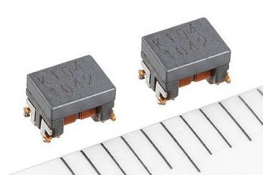
Fig. 4 Common-mode chokes are useful landmarks when tracing differential signal pairs.#
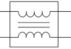
Fig. 5 The component marking and datasheet distinguish a choke from other magnetic components.#
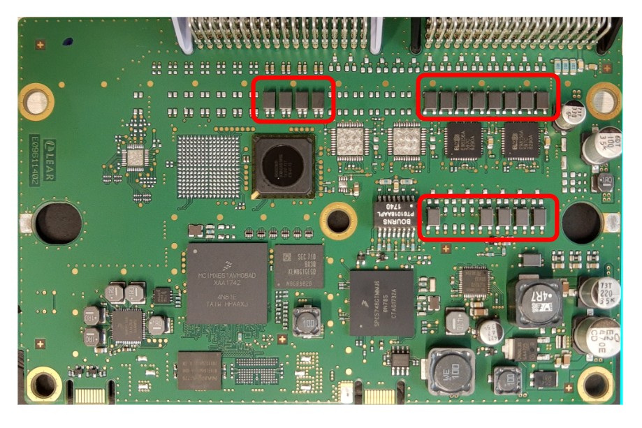
Fig. 6 Trace both sides of a magnetic component to determine its role in the interface.#
Ethernet magnetics may provide isolation and filtering, while the required coupling network depends on the PHY and Ethernet variant. Distinguish multi-pair Ethernet from single-pair automotive Ethernet using the PHY documentation and board routing.
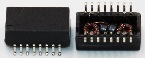
Fig. 7 Ethernet magnetics support identification of the physical interface.#
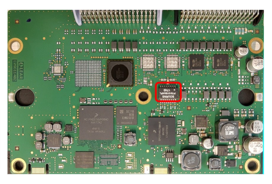
Fig. 8 A connector and its associated magnetics should be traced back to the PHY.#
Identify Integrated Circuits#
Record the full top marking, manufacturer logo, package, and nearby circuitry. Search individual marking strings against manufacturer datasheets, marking guides, reference designs, and errata. A short top code can identify several unrelated parts; confirm the candidate against its pin functions and connections.
For processors, establish the exact family, package variant, instruction set, internal memory, boot options, and debug interface. For custom-marked devices, retain the evidence supporting a family identification and mark unresolved details explicitly.
Communication Transceivers#
A transceiver connects a protocol controller’s logic-level signals to the electrical bus. Follow the signal path from the external connector through protection and filtering to the transceiver, then to the processor or communication controller.
CAN#
A high-speed CAN transceiver typically connects controller-side TXD/RXD signals to CAN_H/CAN_L. The MCU’s CAN controller implements framing and arbitration; the transceiver implements the physical interface. Examples include the Microchip MCP2551, NXP TJA1050, and CAN FD-capable TJA1441 families. Check the exact part’s supply, I/O voltage, mode pins, and package pinout; similar packages do not guarantee interchangeable wiring [NXPSemiconductors21].
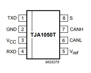
Fig. 9 A transceiver pinout links the bus signals, processor-side signals, supply, and operating-mode control.#
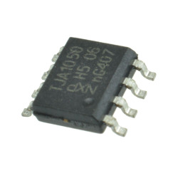
Fig. 10 Use the component marking to select the correct datasheet.#
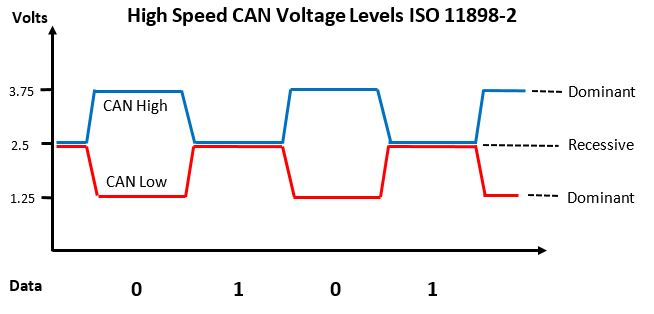
Fig. 11 Electrical bus signalling and the processor’s logic-level interface must be distinguished.#
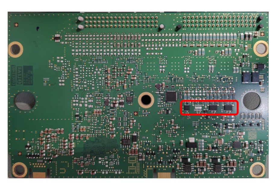
Fig. 12 Trace the transceiver’s logic pins to identify the processor interface.#
Other Interfaces#
Interface |
What to establish from the hardware |
|---|---|
Automotive Ethernet |
PHY variant, single-pair routing, coupling network, and processor-side interface |
FlexRay |
Bus driver, differential pair, channel assignment, and enable/standby control |
LIN |
Single-wire bus connection, LIN transceiver, and UART-style processor interface |
Single-Wire CAN (SWCAN) |
Matching SWCAN transceiver, voltage levels, and wake-up behaviour; a high-speed two-wire CAN transceiver is not a general substitute |
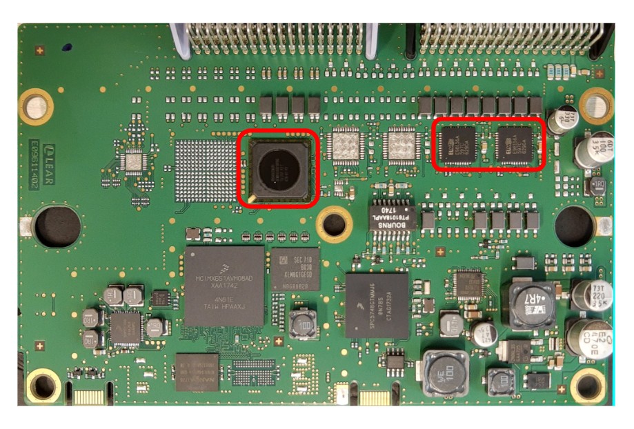
Fig. 13 A controller can expose several physical networks through separate transceivers.#
Non-Volatile Memory#
Identify the memory technology before choosing a reader or interpreting a dump. Package size alone does not identify the interface.
Memory |
Typical role |
Acquisition considerations |
|---|---|---|
MCU internal flash |
Bootloader, application, configuration |
Access depends on the MCU’s debug/boot interfaces and readout protection |
SPI/QSPI NOR flash |
Boot code, executable images, filesystems |
Confirm pinout, voltage, addressing mode, and whether the processor drives the bus during reading |
Raw NAND flash |
Larger firmware images and filesystems |
Requires the device’s NAND interface and treatment of spare/OOB bytes, ECC, and bad blocks |
eMMC |
Managed storage for larger embedded systems |
Uses an MMC interface and an internal flash controller; record the relevant partitions |
EEPROM |
Configuration, calibration, counters, learned values |
Confirm the serial interface and preserve the original contents before modification |
Raw NAND is not generally read using SDIO. Separate it from managed NAND products such as eMMC when selecting acquisition hardware and reconstructing the storage layout [MicrochipTechnology] [ATPElectronics].
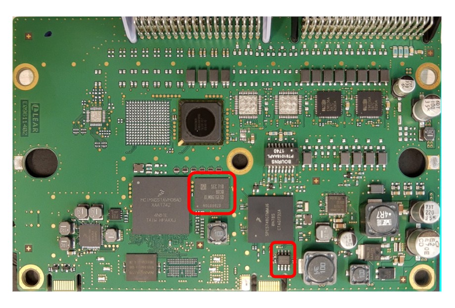
Fig. 14 Memory identification connects physical acquisition options to the firmware and configuration data they may expose.#
System Basis Chips#
A system basis chip (SBC) combines support functions such as voltage regulation, wake-up handling, watchdog supervision, and sometimes CAN or LIN transceivers. Determine which functions are present in the actual part and how the MCU configures them. The SBC can explain why a processor fails to start, resets periodically, or leaves a bus interface in standby.
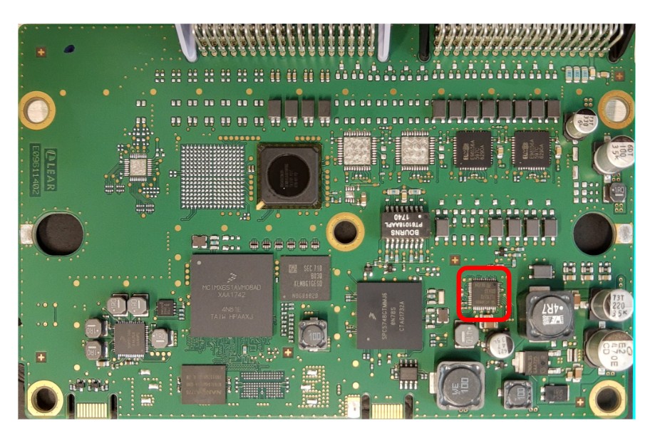
Fig. 15 SBC connections link power, reset supervision, and communication-interface state.#
Hardware Analysis Output#
Record an annotated board photograph, component inventory, connector pinout, power-domain map, and the processor-to-memory and processor-to-transceiver connections. For each debug or acquisition interface, distinguish a candidate footprint from an electrically identified interface and an interface whose access has actually been tested.
This map determines the firmware acquisition route and supplies the processor, memory, and peripheral context needed to interpret the resulting binary.